Moore’s Law observes that the number of transistors on a chip doubles every two years. Based on this law, the development of the computer processors started in the year 1971. Let’s take a look at the journey so far.
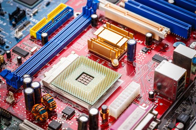
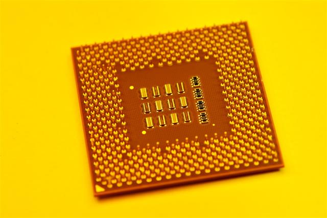
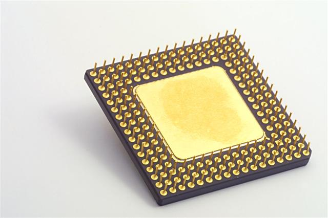
Today, computers are a part of our lifestyle, but the first computer that was used was developed at the University of Pennsylvania in the year 1946! It had an ENIAC (Electronic Numerical Integrator And Computer) processor. The reprogramming feature that is so extensively used today, was introduced by Alan Turing and John von Neumann with their teams. The von Neumann architecture is the basis of modern computers.
From the development of the first microprocessor – Intel’s 4004 to the latest ones – the microprocessors have come a long way. Here, we look into the story so far.Chips Till Date
1971 – Intel 4004
» It was designed by Federico Faggin and Ted Hoff of Intel and Masatoshi Shima of Busicom, and it was launched on November 15,1971.
» It consisted of 2300 transistors with pMOS technology.
» The total number of instructions were 46. The designed clock speed was 1 MHz while only 740 kHz was achieved.
1972 – Intel 8008
» Also known as MCS-8, it was launched in April 1972.
» It was developed by Victor Poor and Harry Pyle of CTC, and Ted Hoff, Faggin, Stanley Mazor and Hal Feeney from Intel.
» It was made up of 3500 transistors. However, it was slower than its predecessor 4004.
» The clock speed was 0.5 MHz with the total number of instructions being 48.
| For the first time it was used in personal computers, Micral and SCELBI. |
1974 – Intel 8080
» Launched in April 1974, it was developed by Faggin, Mazor and Masatoshi Shima.
» The clock speed increased to 2 MHz, it was built on nMOS technology and used 6000 transistors.
» The major development was the separation of address (16-bit) and data (8-bit) bus. It also supported 256 I/Os.
| It was used in the computers MITS Altair 8800 and IMSAI 8080. Space Invaders (arcade video game) also used 8080 as the main processor. |
1974 – Motorola 6800
» This processor developed by Motorola had no I/O ports.
» Memory-mapped input-output were used as I/Os.
» The clock speed was only 2 MHz with the instruction set consisting of 72 instructions.
» It was for the first time that HCF (Halt and Catch Fire) opcode was used, that made the processor unresponsive to any interrupts till it was reset.
1977 – Intel 8085
» Unlike the other processors developed so far, this one was also used as a microcontroller working on +5V supply.
» It was the first time that von Neumann architecture was used.
» It was built with 6500 transistors and used nMOS technology.
» The instruction set consisted of 256 instructions.
| The radiation-hardened version was used in NASA and ESA space expeditions. |
1978 – Intel 8086
» The designed clock speed was 10 MHz.
» The development team for architecture consisted of Stephen P. Morse and Bruce Ravenel. Logic was designed by Jim McKevitt, John Bayliss, and William Pohlman was the project manager.
| This was first used in the microcomputer Mycron 2000. |
1979 – Intel 8088
» 8088 was based on the new HMOS technology and was launched on 1 July.
» It came in 40-pin DIP as well as PLCC (plastic leaded chip carrier) package.
» However, the data path was only 8-bit. The designed frequency was 10 MHz.
The original IBM PC was based on 8088.
1987 – SPARC
» This processor was developed by Sun Microsystems.
» It had a clock speed of 40 MHz.
» It was made up of 1.8 million transistors with 256 IO pins.
| Fujitsu’s K Computer is ranked number 1 in the world’s fastest 500 supercomputers as per TOP500 list ratings. It used SPARC. |
1991 – Am386
» This AMD (Advanced Micro Devices) processor had striking resemblance to the Intel 80386 version x86 processors.
» With a clock speed of 40 MHz and 32-bit data bus, the processor was a competitor to Intel.
| The excellent performance of AMD’s floating point unit made it the second best choice (after Intel) for many manufacturers. |
1993 – Pentium Processor
» The Pentium family started with the launch of the P5 processor.
» It came in two models – 510-pin version with 60 MHz clock speed and 567-pin version with a clock speed of 66 MHz.
» Launched on March 22, it was built with 3.1 million transistors.
» This 32-bit processor was the most advanced processor used in many computers that were manufactured at that time.
| It was the first superscalar x86 microarchitecture that could execute two instructions simultaneously, thus speeding up the processor and reducing computing time. |
1995 – Pentium Pro
» This was the first processor of the Pentium II series.
» This latest entrant came in an unconventional MCM (ceramic multi-chip module) 387 pins packaging.
» With a clock speed of 200 MHz, it was built to run in quad as well as dual processor configurations.
» About 5.5 million transistors were used to build this processor.
» It did not have an MMX instruction set.
| This processor was used in ASCI Red that delivered teraFLOP (one trillion floating-point operations in one second) performance. |
1997 – Pentium II
» Launched on 7 May, the Pentium II family had a vast range of processors to offer.
» The clock speed was increased gradually with every model launched to up to 450 MHz.
» Unlike the traditional processors, this one came in a slot or socket module. This made it easy for the computer manufacturers to use it in a limited space.
» Various processors were launched under this family:
- Klamath (233 and 266 MHz)
- Deschutes (333 MHz)
- Pentium II Overdrive (300 or 333 MHz)
- Tonga (First mobile Pentium II)
- Dixon (Considered to be the fastest Pentium II)
| It had a removable heatsink/fan combination that reduced the problem of heat dissipation. |
1999 – Pentium III
» This Pentium II successor was launched on 26 February.
» The advancement from the previous model was the addition of the SSE instruction that accelerated the floating point calculations.
» On the similar lines as Pentium II, this processor was launched in Celeron (Low-end version) and Xeon (High-end version).
» The list of processors under this family are:
- Katmai: Clock speed of 450 MHz and uses 9.5 million transistors
- Coppermine: Clock speed of up to 1 GHz
- Coppermine T: Only Coppermine model with an integrated heatsink (IHS)
- Tualatin: Clock speed up to 1.4 GHz and 0.13 µm process
| PSN (Processor Serial Number) was introduced in the manufacturing process that created the processor’s unique identity, which was the first instance. |
1999 – Athlon
» AMD launched Athlon on June 23. It was built using 37 million transistors and achieved a clock speed of about 800 MHz.
» It was packaged in a unique PGA (Pin Grid Array) 453-pin packaging.
» Athlon was a legitimate competitor to Intel Pentium III because it was faster.
» It was the first processor to reach the speed of 1 GHz.
| Enhanced 3DNow! was first introduced, which increased the speed up to 2-4 times. |
2000 – Pentium IV
» Intel’s new single core processor family in the market was the Pentium IV processor that achieved a clock speed between 1.3 GHz to 3.08 GHz.
» The 423-pin processor came in an OLGA (Organic Land Grid Array) and PPGA (Plastic Pin Grid Array) type packaging.
» The processors under this family are:
- Willamette: Clock speed of 1.4 and 1.5 GHz and 180 nm process
- Northwood: Clock speed up to 2.2 GHz and 130 nm die
- Pentium 4-M: Built for Mobile use with TDP of 35 watts
- Mobile Pentium 4: Built for laptop use with increased bus speed of 33 MHz
- Gallatin: Die of 130 nm and an added 2 MB level 3 cache
- Prescott: Die of 90 nm and hyper-threading that speeds up processes such as video editing
- Prescott 2M: Clock speed of 3.8 GHz and 90 nm process
- Cedar Mill: Die of 65 nm
| The NetBurst architecture was first used in the processors under this family. |
2003 – Pentium M
» This processor was a mobile single-core processor from Intel.
» It was designed with a clock speed of 2.26 GHz.
» Two processors were developed under this family, namely:
- Banias: Clock speed of 1.7 GHz and TDP of 24.5 watts
- Dothan: Die of 90 nm and clock speed of 2.1 GHz; TDP is reduced to 21 watts
| This processor was used for the first time in Intel Carmel notebook under Centrino brand. |
2006 – Core 2
» Intel Core 2 brand, launched on July 27, 2006, was also known as E6320.
» The clock speed was achieved up to 3.5 GHz.
» The processors launched under this family were single-core, dual-core and quad-core.
» The processor has been dropped from the price list since 2011.
» The processors under this brand for desktops are:
- Conroe: Die of 65 nm (dual)
- Allendale: Die of 65 nm (dual)
- Wolfdale: Die of 45 nm (dual)
- Conroe XE: Die of 65 nm (dual)
- Allendale XE: Die of 65 nm (quad)
- Wolfdale XE: Die of 45 nm (dual)
- Kentsfield: Die of 65 nm (quad)
- Yorkfield: Die of 45 nm (quad)
» The processors under this brand for laptops are:
- Merom: Die of 65 nm (dual)
- Penryn: Die of 45 nm (dual)
- Merom XE: Die of 65 nm (dual)
- Penryn XE: Die of 45 nm (quad and dual)
- Merom-L: Die of 65 nm (single)
- Penryn-L: Die of 45 nm (single)
| The processor was capable of saving battery power by lowering the clock speed. |
The Latest
The microprocessor technology has come a long way since the launch of 4004. The chip size has reduced, the clock speed has increased and the caches have further increased. The latest processors that have achieved this are:
Sandy Bridge
This Intel microarchitecture-based products were launched in 2011. It has achieved a 32-nanometer die manufacturing. It includes Intel Quick sync that is a hardware support for video encoding and decoding. There is also an improved 256-bit/cycle ring bus connect that interconnects the different parts of the processor. The transistor count used in this processor reaches up to 2.27 billion. This is the successor to the Nehalem microarchitecture family that achieved 45 nm manufacturing. The clock speed designed is 3.6 GHz. Intel recalled 67-series motherboards that had Cougar Point Chipset due to some hardware issue. The series under this family are:
- Pentium: Clock speed up to 3.0 GHz
- Celeron: Clock speed up to 3.0 GHz
- Core i3: Clock speed up to 2.5 GHz
- Core i5: Clock speed up to 3.4 GHz
- Core i7: Clock speed up to 3.3 GHz
- Core i7 Extreme: Clock speed up to 3.8 GHz
| It has a vPro feature that can delete the information on a hard disk and the commands for this can be sent through 3G signals, Ethernet or Internet. |
Ivy Bridge
An amazing 22-nm die processor named Ivy Bridge was announced by Intel in 2011, but it was introduced in the market on April 29, 2012. Reduced die is possible due to the use of the 3D (tri-gate) transistors. The 3D transistors reduce the power consumption to almost 50% less than the 2D ones. It also includes special support for PCI Express and also better graphics with DirectX 11. The clock speed is about 3.80 GHz. They are reported to have 20ºC higher temperature than Sandy Bridge. The desktop models under this family are:
- Core i3 Series: Clock speed up to 3.4 GHz
- Core i5 Series: Clock speed up to 3.8 GHz
- Core i7 Series: Clock speed up to 3.5 GHz
The mobile models for under this family are:
- Core i3 Series: TDP of 14W
- Core i5 Series: TDP of 14W
- Core i7 Series: TDP of 14W to 45W
| It is one of the ‘tick’ versions of Sandy Bridge. |
The Future
The future processors that are expected to be launched in the 2013 are very promising. Here’s a sneak preview.
» Haswell is being developed with a further shrunken die of 22 nm.
» Broadwell is announced to have a 14-nm die with Multi-chip packaging design that will be used.
» Skylake processors are expected to be available by 2015 with 14 nm process.
» The latest one to join this league is Skymont that will have a die of 10 nm.
» There are also indications of development of processors with die as small as 5 nm!
From the clock frequency of 1 MHz to about 3 GHz, the processor technology has come a long way. The die has shrunken to 22 nm and the miniaturization is still on. All these signs point to a brighter future for processors, which will come to benefit everyone.


Reference:


